Security image sensor
Development
The core function of image sensor is to convert natural light signals into electrical signals, so it can be called charge coupled device (CCD). Common image sensors are CCD and CMOS. In the era of analog standard definition for security video monitoring, CCD image sensor is the main, and Sony 639,673,811 is the representative, which is the classic product in the era of analog monitoring.
With the development of network technology and chip technology, security video surveillance has entered the era of network HD. CCD image sensor products are gradually eliminated, and CMOS image sensor has become the main. Now it is difficult to see the security camera equipped with CCD image sensor. Since 2010, the market share of CCD has been declining, and Sony stopped producing CCD sensors in 2017. In other image and video fields, such as machine vision, medical and so on, CCD image sensors can also be seen, especially high-level scanners and military equipment are still monopolized by CCD.
Classification
Image sensors are divided into CCD and CMOS.
CCD is charge coupled device. In charge coupled device, the charge data of each pixel in each row of the sensor will be transferred to the next pixel in turn, which is output by the bottom part, and then amplified by the amplifier at the edge of the sensor.
CMOS is a kind of complementary metal oxide semiconductor. Different from CCD, each pixel in CMOS sensor is adjacent to an amplifier and A / D conversion circuit, which outputs data in a way similar to memory circuit.
CCD sensor technology was invented by two scientists of Bell laboratory in 1969, and CCD image sensor was born in 1971. In 2009, the two scientists won the Nobel Prize in physics for their contributions to the development of CCD.
CMOS technology appeared earlier. It was invented by an engineer of American Express semiconductor company in 1963. At first, it was used as an integrated circuit design process, and then it was used to produce active pixel sensor, namely CMOS image sensor.
In front of the analysis of the CCD and CMOS structure is different, it is because of this difference affects the advantages and disadvantages of the two.
Under the same conditions, CMOS uses relatively few components, so it has lower power consumption and faster data throughput than CCD. At the same time, CMOS has amplifiers on each pixel to read out data separately, which leads to image inconsistency and noise. However, CCD only reads data from one node, so the image has good consistency and less noise.
Compare with CCD&CMOS
| item | Resolution | Sensitivity | SNR | Integration | Power | Cost | Speed |
| CCD | better | better | |||||
| CMOS | better | lower | lower | better |
Brand
In addition to traditional international brands, such as Sony, Samsung, OV and aptina, domestic smartsens, Starway, Taiwan’s pixart and crystalline SOI products are also very good in the image sensor market.
Common security video surveillance image sensors and brands (last updated on 2021.4.27)
| Brand/Model | Specification |
|---|---|
| SONY | |
| IMX290 | 1/2.8′,2.9µm,2.0MP,Starvis,DOL HDR,120fps |
| IMX307 | 1/2.8′,2.9µm,2.0MP,Starvis,DOL HDR,60fps |
| IMX327 | 1/2.8′,2.9µm,2.0MP,Starvis,DOL HDR,60fps |
| IMX385 | 1/2′,3.75µm,2.0MP,DOL HDR,120fps |
| IMX123 | 1/2.8′,2.5µm,2.0MP,Starvis,DOL HDR,NIR,120fps |
| IMX335 | 1/2.8′,2.0µm,5.0MP,Starvis,DOL HDR,60fps |
| IMX178 | 1/1.8′,2.4µm,6.3MP,Starvis,60fps |
| IMX274 | 1/2.5′,1.62µm,4K,Starvis,DOL HDR,60fps |
| IMX334 | 1/1.8′,2.0µm,4K,Starvis,DOL HDR,60fps |
| IMX226 | 1/1.7′, 1.85µm,12.4MP, Starvis,40fps |
| IMX415 | 1/2.8′,1.45µm,8.29MP,Starvis,DOL HDR,90fps |
| IMX515 | 1/2.8′,1.45µm,8.46MP,Starvis,DOL HDR,61fps |
| OmniVision | |
| OS08A10 | 1/1.8′,2.0µm,4K,60fps |
| OS05A10 | 1/2.7′,2.0µm,5.0MP,60fps |
| OV4689 | 1/3.0′,2.0µm,2.0MP,90fps |
| OV5658 | 1/3.2′,1.75µm,5.0MP,30fps |
| SmartSens | |
| SOINC | |
| PIXart | |
| Galaxycore | |
| Aptina | |
| Panasonic | |
| STMicroelectronics | |
| SKhynix | |
| Canon | |
| Toshiba | |
| infineon | |
| Ams | |
| Kodak | |
| 思比科 | |
| BYD | |
| 锐芯 | |
| 长光辰芯 |
Main technical parameters
Low light: starvis, snr1s
Wide dynamic: WDR / dol-hdr / BLC
IR: NIR
Pixels: resolution, target size
Global shutter
Sensitivity, SNR
power waste
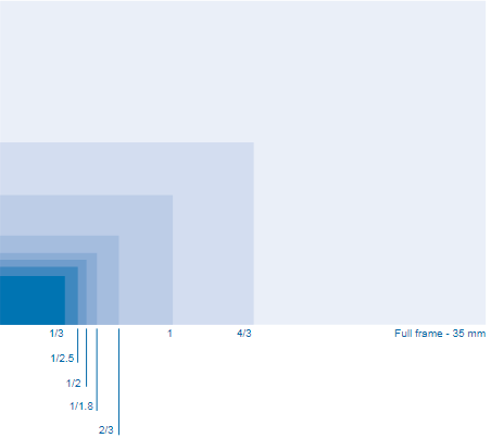
Common image sensor size
| Sensor size | Diagonal length(mm) | width(mm) | height(mm) |
| 1/3″ | 6 | 4.8 | 3.2 |
| 1/2.5″ | 7.182 | 5.760 | 4.290 |
| 1/2″ | 8 | 6.4 | 4.8 |
| 1/1.8″ | 8.933 | 7.176 | 5.319 |
| 2/3″ | 11 | 8.8 | 6.6 |
| 1″ | 16 | 12.8 | 9.6 |
| 4/3″ | 22.5 | 18.8 | 13.5 |
| Full frame-35mm | 43.3 | 36 | 24 |
Technology development (take Sony as an example)
In 2007, column parallel a / D conversion circuit equivalent CMOS image sensors. Each vertical row of pixels has an A / D converter, arranged in parallel. In this arrangement, the analog signal read from the vertical signal line can be directly transmitted to the ADC of each row through the minimum distance, which reduces the image quality loss caused by the noise entering the signal during the analog transmission, and speeds up the readout of the signal. The noise is also reduced by double noise elimination.
In 2009, back illuminated CMOS image sensor. Receiving light from the back of silicon substrate increases the light input and loss, and improves the sensitivity.
In 2012, stacked CMOS image sensors. Stack structure, pixel part and circuit part are layered to achieve higher resolution, more functions and more compact structure.
2015, stacked CMOS image sensor with Cu Cu connector. The pixel chip and logic circuit chip are connected by copper chip, without providing electrical connection through the pixel chip or special area, so as to improve the production efficiency of good chip, produce smaller size sensors and expand more functions.
Now, AI sensor. Add AI function on the traditional sensor logic chip layer to directly output structured data or optional AI model. Real edge AI. Sony’s first AI CMOS sensor imx500 / 501.
At the end of the article, two questions are put forward, which are also discussed more at present.
As an image sensor, which is more important, the big bottom or the high pixel?
Some photography lovers prefer the SLR of CCD sensor, think CCD is better, personal preference or others, worship or Metaphysics?
Leave a Reply
Want to join the discussion?Feel free to contribute!